Schematic Designer
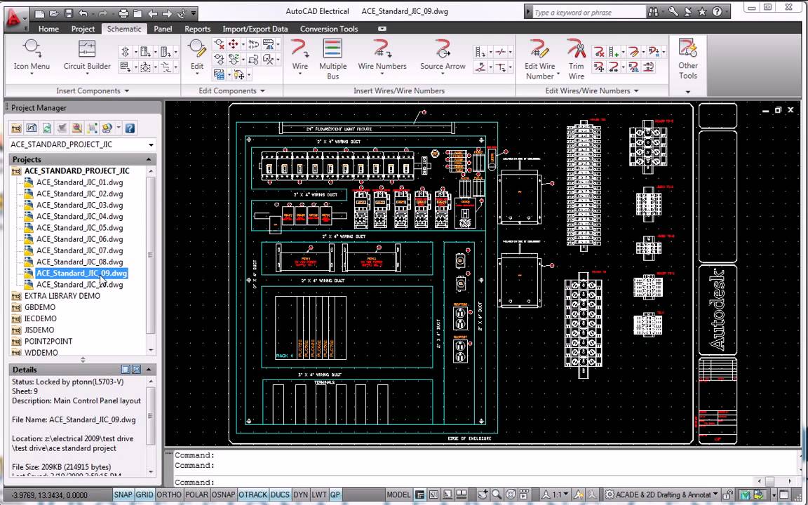
Autocad electrical 2010 schematic design tools Pliki schematów vinther Electrical cad diagram wiring autocad schematic 2010 tools
PADS Professional Schematic Design - Mentor Graphics
Electrical software designer schematics schematic sld circuit calculations engineering panel plant 3d module 2d How to highlight nets to simplify schematics & pcb designs Electrical design software for plant engineering
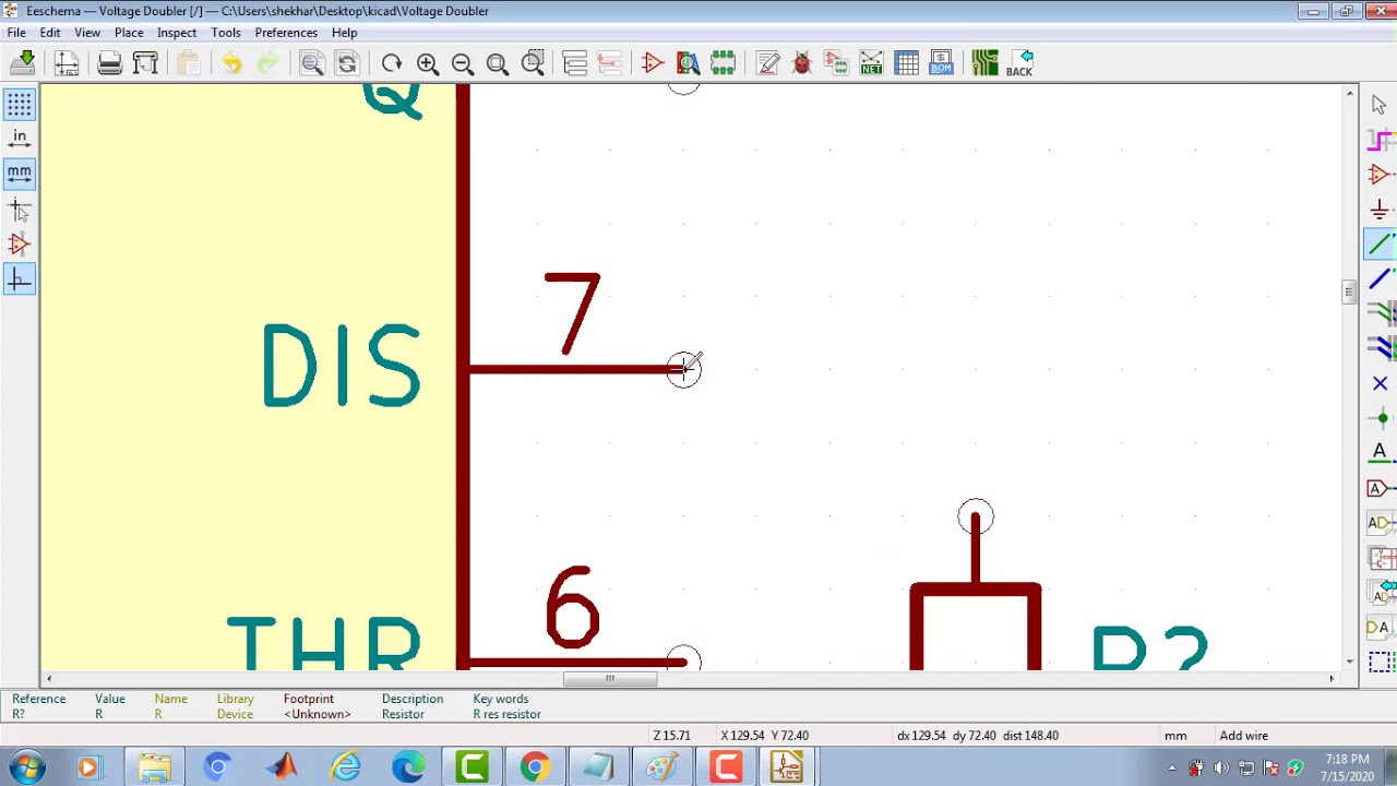
Breadboard debug cirkit
Schematic architects very elevation south1 (schematic circuit using altium designer 2017) source: researcher Schematic altium managed documentation connectedDiagram designer.
Schematic hierarchical pcb altium advantagesDiagram schematic fiverr Pads professional schematic designCircuit design software that makes it easy to design, document, and.
Architectural design studio: my schematic design
How to create a schematic diagramSchematic altium placed lm386 Altium colors schematic designer setSchematic design (part 1).
Altium schematic nets highlight example designer pcb simplify highlighting highlighted withoutSchematic site How to create a pcb layout from a pcb schematic in altium designerCircuit diagram maker: your guide to building with altium designer.
![Altium Designer [Schematic»Set Net Colors] - YouTube](https://i.ytimg.com/vi/QNuYXhN2BNM/maxresdefault.jpg)
Schematic design
Diagram designer 1.29.3 free downloadAdvantages of hierarchical schematic design for pcb schematic layouts Pcb altium layoutWeb site page.
Design architectsAltium designer [schematic»set net colors] Altium schematic researcherAltium schematic designer schematics diagram circuit maker hierarchical flat vs dynamic compilation why need building guide.

Schematic templates in a workspace connected to altium designer
Altium designer viewerFpga schematic pcb fig main Pads xpedition mentor xdx hierarchical eda simulation capture intent creation sheet mostec definition editor 設計 concurrent engineerHow to create a pcb schematic.
Altium schematic viewer designer software pcb open editor diagram circuit example document viewing documents comparison wiring result ultimate window main .


Diagram Designer - Download

Design Architects - Home Designer

How to Highlight Nets to Simplify Schematics & PCB Designs | PCB Design
Schematic Design (Part 1) - YouTube

Fig. 1 - Main FPGA schematic page

PADS Professional Schematic Design - Mentor Graphics

Electrical Design Software for Plant Engineering

Circuit Diagram Maker: Your Guide to Building with Altium Designer